Identifying EMI-ESD Symbols and Layout on schematic diagram and PCB board
EMI-Electromagnetic Interference and ESD-Electrostatic Discharge is pack in tiny chips called by many technician as Crystal IC for it glows like a crystal glass.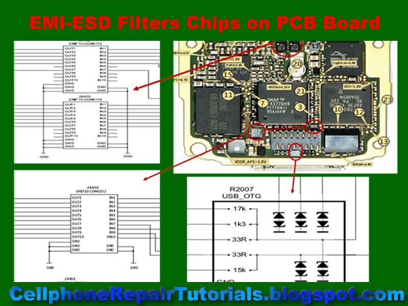
EMI-ESD filter are used to protect a certain circuit from hazardous Electromagnetic Interference and Electrostatic Discharge.
Electromagnetic Interference cause by elecromagnetic machines like like a chainsaw, an electric blower and other things that has high frequency levels.
Electrostatic Discharge (ESD)- a human body is a potential source of electrostatic and can cause damage, especially to semiconductor devices when touching it.
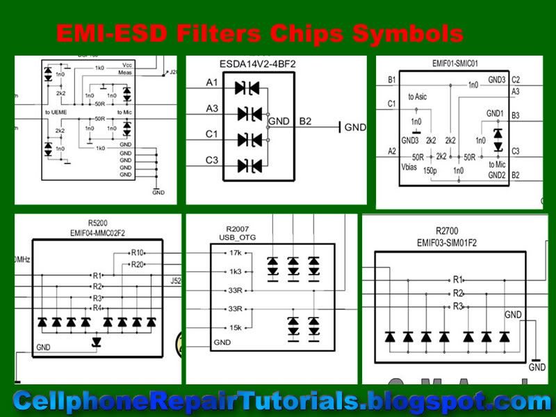
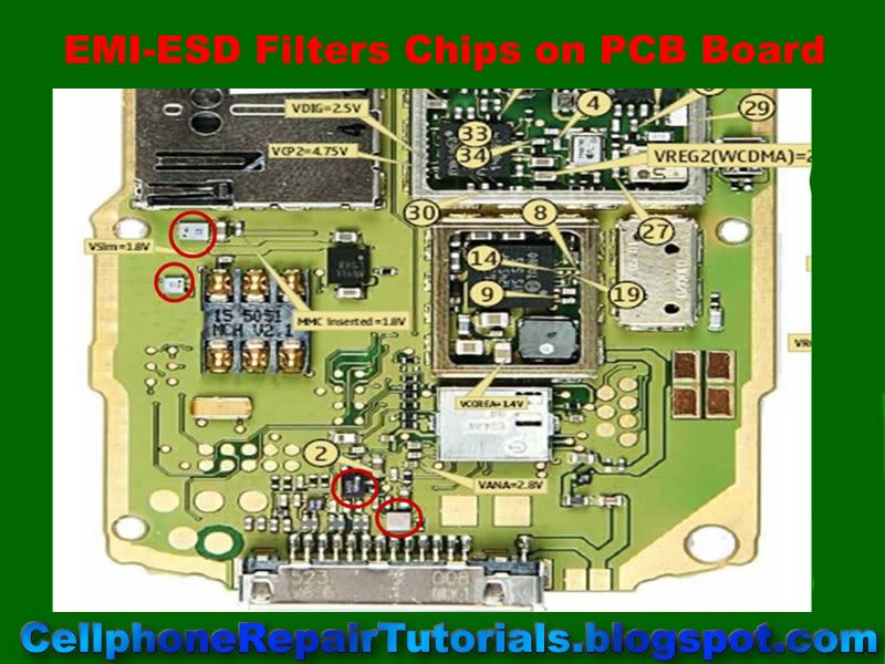
EMI-ESD Filters can be easily breakdown and busted when those two elements occurs. It often used in Keypads circuit, Display circuit, USB (Universal Serial Bus)Interface circuit, Removable Flash Memory Devices circuit and other Interface that is prone to ESD and EMI hazards.
EMI-Electromagnetic Interference and ESD-Electrostatic Discharge is pack in tiny chips called by many technician as Crystal IC for it glows like a crystal glass.

EMI-ESD filter are used to protect a certain circuit from hazardous Electromagnetic Interference and Electrostatic Discharge.
Electromagnetic Interference cause by elecromagnetic machines like like a chainsaw, an electric blower and other things that has high frequency levels.
Electrostatic Discharge (ESD)- a human body is a potential source of electrostatic and can cause damage, especially to semiconductor devices when touching it.


EMI-ESD Filters can be easily breakdown and busted when those two elements occurs. It often used in Keypads circuit, Display circuit, USB (Universal Serial Bus)Interface circuit, Removable Flash Memory Devices circuit and other Interface that is prone to ESD and EMI hazards.

0 comments:
Post a Comment